- Home
- About
- Products
- Product Testing
- Application
- Services
- Information
- Contact
- All
- Product Name
- Product Keyword
- Product Model
- Product Summary
- Product Description
- Multi Field Search
 English
Views: 1215 Author: Site Editor Publish Time: 2020-10-04 Origin: Site
PCB is almost inseparable from the electronic equipment we can see, from electronic watches, calculators, general computers, to computers, communication electronic equipment, military weapon systems. As long as there are integrated circuits and other electronic components, PCB is used for electrical interconnection between them. In addition to fixing various small parts, it provides mechanical support for fixed assembly of various electronic components such as integrated circuit, realizes wiring and electrical connection or electrical insulation between various electronic components such as integrated circuit, and provides required electrical characteristics, such as characteristic impedance and so on. At the same time, it provides the solder resist pattern for automatic soldering, and the identification characters and graphics for component insertion, inspection and maintenance. With the increasing complexity of electronic equipment, more and more parts are needed, so the circuits and parts on the PCB are becoming denser.
The keyboard of the general computer has a soft film (flexible insulating substrate), printed with silver-white (silver paste) conductive patterns and key graphics. Because this pattern is obtained by the common screen miss printing method, this PCB is called a flexible silver paste printed circuit board. The printed circuit boards on various computer mainboards, video cards, network cards, modems, sound cards and household appliances are different. The base material used is made of paper base (commonly used for single-sided) or glass cloth base (commonly used for double-sided and multi-layered), pre impregnated with phenolic or epoxy resin, one or both sides of the surface layer are pasted with copper sheet, then laminated and solidified. This kind of circuit board is called rigid board. Remanufactured printed wiring board is rigid printed wiring board. The single-sided printed wiring board refers to a printed circuit pattern on one side, and the double-sided printed wiring board refers to a printed circuit pattern on both sides. Double-sided board refers to a printed wiring board formed by double-sided interconnection through metallization of holes. If a printed circuit board with one double side as the inner layer, two single side as the outer layer or two double sides as the inner layer and two single side as the outer layer is used, the printed circuit board which is alternately connected by the positioning system and the insulating bonding material and the conductive graphics are interconnected according to the design requirements will become a four or six layer printed circuit board, also known as a multi-layer printed circuit board. There are more than 100 layers of practical printed circuit boards.
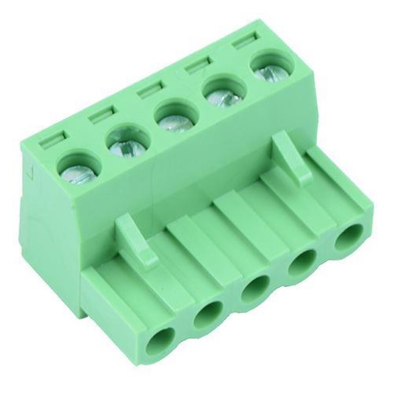
PCB terminal uses the edge connector to connect two PCBs. When PCB terminal is connected, insert the cable connector on one PCB into the appropriate slot on the other PCB. There are many exposed copper pads on the side connector, which are actually part of electrical cable.
PCB production process is more complex, it involves a wide range of processes. There are common chemical reactions, photochemistry, electrochemistry, thermochemistry, CAD and other aspects of knowledge during the machining of PCB terminal. As the production process of PCB terminal is a kind of discontinuous assembly line, any problem in any link will cause the whole line to stop production or a large number of scrapped consequences. If the PCB is scrapped, it can not be recycled.